- My Shodhganga
- Receive email updates
- Edit Profile

Shodhganga : a reservoir of Indian theses @ INFLIBNET
- Shodhganga@INFLIBNET
- Anna University
- Faculty of Science and Humanities
Items in Shodhganga are licensed under Creative Commons Licence Attribution-NonCommercial-ShareAlike 4.0 International (CC BY-NC-SA 4.0).

Thank you for visiting nature.com. You are using a browser version with limited support for CSS. To obtain the best experience, we recommend you use a more up to date browser (or turn off compatibility mode in Internet Explorer). In the meantime, to ensure continued support, we are displaying the site without styles and JavaScript.
- View all journals
- Explore content
- About the journal
- Publish with us
- Sign up for alerts
- Published: 30 March 2023
Unravelling crystal growth of nanoparticles
- Binbin Luo 1 na1 ,
- Ziwei Wang ORCID: orcid.org/0000-0002-2651-0813 2 na1 ,
- Tine Curk 3 ,
- Garrett Watson 3 ,
- Chang Liu 1 ,
- Ahyoung Kim ORCID: orcid.org/0000-0002-7366-038X 1 ,
- Zihao Ou ORCID: orcid.org/0000-0003-2987-7423 1 ,
- Erik Luijten ORCID: orcid.org/0000-0003-2364-1866 2 , 3 , 4 , 5 , 6 &
- Qian Chen ORCID: orcid.org/0000-0002-1968-441X 1 , 7 , 8 , 9
Nature Nanotechnology volume 18 , pages 589–595 ( 2023 ) Cite this article
9311 Accesses
6 Citations
73 Altmetric
Metrics details
- Imaging techniques
- Nanoparticles
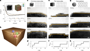
Crystal growth from nanoscale constituents is a ubiquitous phenomenon in biology, geology and materials science. Numerous studies have focused on understanding the onset of nucleation and on producing high-quality crystals by empirically sampling constituents with different attributes and varying the growth conditions. However, the kinetics of post-nucleation growth processes, an important determinant of crystal morphology and properties, have remained underexplored due to experimental challenges associated with real-space imaging at the nanoscale. Here we report the imaging of the crystal growth of nanoparticles of different shapes using liquid-phase transmission electron microscopy, resolving both lateral and perpendicular growth of crystal layers by tracking individual nanoparticles. We observe that these nanoscale systems exhibit layer-by-layer growth, typical of atomic crystallization, as well as rough growth prevalent in colloidal systems. Surprisingly, the lateral and perpendicular growth modes can be independently controlled, resulting in two mixed crystallization modes that, until now, have received only scant attention. Combining analytical considerations with molecular dynamics and kinetic Monte Carlo simulations, we develop a comprehensive framework for our observations, which are fundamentally determined by the size and shape of the building blocks. These insights unify the understanding of crystal growth across four orders of magnitude in particle size and suggest novel pathways to crystal engineering.
This is a preview of subscription content, access via your institution
Access options
Access Nature and 54 other Nature Portfolio journals
Get Nature+, our best-value online-access subscription
24,99 € / 30 days
cancel any time
Subscribe to this journal
Receive 12 print issues and online access
251,40 € per year
only 20,95 € per issue
Buy this article
Purchase on Springer Link
Instant access to full article PDF
Prices may be subject to local taxes which are calculated during checkout
Kinetic pathways of crystallization at the nanoscale
Zihao Ou, Ziwei Wang, … Qian Chen

Observing crystal nucleation in four dimensions using atomic electron tomography
Jihan Zhou, Yongsoo Yang, … Jianwei Miao

Crystal dissolution by particle detachment
Guomin Zhu, Benjamin A. Legg, … James J. De Yoreo
Data availability
All data are available in the Article or the Supplementary Information .
Code availability
Additional codes for image processing, particle tracking and simulations are available from the corresponding authors upon request.
Liu, Y., Wang, X. & Ching, C. B. Toward further understanding of lysozyme crystallization: phase diagram, protein−protein interaction, nucleation kinetics, and growth kinetics. Cryst. Growth Des. 10 , 548–558 (2010).
Article CAS Google Scholar
García-Ruiz, J. M. & Otálora, F. in Handbook of Crystal Growth 2nd edn (ed Rudolph, P.) 1−43 (Elsevier, 2015).
De Yoreo, J. J. et al. Crystallization by particle attachment in synthetic, biogenic, and geologic environments. Science 349 , aaa6760 (2015).
Article Google Scholar
Boles, M. A., Engel, M. & Talapin, D. V. Self-assembly of colloidal nanocrystals: from intricate structures to functional materials. Chem. Rev. 116 , 11220–11289 (2016).
Auyeung, E. et al. DNA-mediated nanoparticle crystallization into Wulff polyhedra. Nature 505 , 73–77 (2014).
Ye, X. et al. Quasicrystalline nanocrystal superlattice with partial matching rules. Nat. Mater. 16 , 214–219 (2017).
Li, D. et al. Direction-specific interactions control crystal growth by oriented attachment. Science 336 , 1014–1018 (2012).
Pierret, R. F. in Semiconductor Device Fundamentals (Addison-Wesley, 2003).
Einstein, T. L. & Stasevich, T. J. Epitaxial growth writ large. Science 327 , 423–424 (2010).
Zhang, Z. & Lagally, M. G. Atomistic processes in the early stages of thin-film growth. Science 276 , 377–383 (1997).
Ju, G. et al. Coherent X-ray spectroscopy reveals the persistence of island arrangements during layer-by-layer growth. Nat. Phys. 15 , 589–594 (2019).
Voronkov, V. V. in Growth of Crystals: Volume 10 (ed Sheftal’, N. N.) 1–17 (Springer, 1976).
Brune, H. Microscopic view of epitaxial metal growth: nucleation and aggregation. Surf. Sci. Rep. 31 , 125–229 (1998).
Gasser, U., Weeks, E. R., Schofield, A., Pusey, P. N. & Weitz, D. A. Real-space imaging of nucleation and growth in colloidal crystallization. Science 292 , 258–262 (2001).
Palberg, T. Crystallization kinetics of colloidal model suspensions: recent achievements and new perspectives. J. Phys.: Condens. Matter 26 , 333101 (2014).
Google Scholar
Rossi, L. et al. Cubic crystals from cubic colloids. Soft Matter 7 , 4139–4142 (2011).
Xie, R. & Liu, X.-Y. Controllable epitaxial crystallization and reversible oriented patterning of two-dimensional colloidal crystals. J. Am. Chem. Soc. 131 , 4976–4982 (2009).
Aarts, D. G. A. L., Schmidt, M. & Lekkerkerker, H. N. W. Direct visual observation of thermal capillary waves. Science 304 , 847–850 (2004).
Ou, Z., Wang, Z., Luo, B., Luijten, E. & Chen, Q. Kinetic pathways of crystallization at the nanoscale. Nat. Mater. 19 , 450–455 (2020).
Ross, F. M. Opportunities and challenges in liquid cell electron microscopy. Science 350 , aaa9886 (2015).
Luo, B., Smith, J. W., Ou, Z. & Chen, Q. Quantifying the self-assembly behavior of anisotropic nanoparticles using liquid-phase transmission electron microscopy. Acc. Chem. Res. 50 , 1125–1133 (2017).
Silvera Batista, C. A., Larson, R. G. & Kotov, N. A. Nonadditivity of nanoparticle interactions. Science 350 , 1242477 (2015).
O’Brien, M. N., Jones, M. R., Brown, K. A. & Mirkin, C. A. Universal noble metal nanoparticle seeds realized through iterative reductive growth and oxidative dissolution reactions. J. Am. Chem. Soc. 136 , 7603–7606 (2014).
Lu, F., Yager, K. G., Zhang, Y., Xin, H. & Gang, O. Superlattices assembled through shape-induced directional binding. Nat. Commun. 6 , 6912 (2015).
Zhang, Z., Detch, J. & Metiu, H. Surface roughness in thin-film growth: the effect of mass transport between layers. Phys. Rev. B 48 , 4972–4975 (1993).
Ganapathy, R., Buckley, M. R., Gerbode, S. J. & Cohen, I. Direct measurements of island growth and step-edge barriers in colloidal epitaxy. Science 327 , 445–448 (2010).
Parsegian, V. A. Van der Waals Forces: A Handbook for Biologists, Chemists, Engineers, and Physicists (Cambridge Univ. Press, 2005).
Wang, S. C. & Ehrlich, G. Adatom motion to lattice steps: a direct view. Phys. Rev. Lett. 70 , 41–44 (1993).
Venables, J. A., Spiller, G. D. T. & Hanbucken, M. Nucleation and growth of thin films. Rep. Prog. Phys. 47 , 399–459 (1984).
Tersoff, J., Denier van der Gon, A. W. & Tromp, R. M. Critical island size for layer-by-layer growth. Phys. Rev. Lett. 72 , 266–269 (1994).
Krug, J., Politi, P. & Michely, T. Island nucleation in the presence of step-edge barriers: theory and applications. Phys. Rev. B 61 , 14037–14046 (2000).
Heinrichs, S., Rottler, J. & Maass, P. Nucleation on top of islands in epitaxial growth. Phys. Rev. B 62 , 8338–8359 (2000).
Krug, J. Four lectures on the physics of crystal growth. Phys. A: Stat. Mech. Appl. 313 , 47–82 (2002).
Slepoy, A., Thompson, A. P. & Plimpton, S. J. A constant-time kinetic Monte Carlo algorithm for simulation of large biochemical reaction networks. J. Chem. Phys. 128 , 205101 (2008).
Clarke, S. & Vvedensky, D. D. Growth kinetics and step density in reflection high‐energy electron diffraction during molecular‐beam epitaxy. J. Appl. Phys. 63 , 2272–2283 (1988).
Schneider, C. A., Rasband, W. S. & Eliceiri, K. W. NIH Image to ImageJ: 25 years of image analysis. Nat. Methods 9 , 671–675 (2012).
Karperien, A. FracLac for ImageJ (Charles Stuart Univ., 2013).
Download references
Acknowledgements
We thank J. Kim for useful discussions. Z.W. gratefully acknowledges support from a Ryan Fellowship and the International Institute for Nanotechnology at Northwestern University. This material is based on work supported by the US Department of Energy, Office of Science, Office of Basic Energy Sciences, Division of Materials Sciences and Engineering, under award nos. DE-SC0020723 and DE-SC0020885. G.W. was supported by the National Science Foundation Graduate Research Fellowship under grant no. DGE-1842165 and T.C. by the EU’s Horizon 2020 programme under Marie Skłodowska-Curie Fellowship no. 845032.
Author information
These authors contributed equally: Binbin Luo, Ziwei Wang.
Authors and Affiliations
Department of Materials Science and Engineering, University of Illinois at Urbana-Champaign, Urbana, IL, USA
Binbin Luo, Chang Liu, Ahyoung Kim, Zihao Ou & Qian Chen
Graduate Program in Applied Physics, Northwestern University, Evanston, IL, USA
Ziwei Wang & Erik Luijten
Department of Materials Science and Engineering, Northwestern University, Evanston, IL, USA
Tine Curk, Garrett Watson & Erik Luijten
Department of Engineering Sciences and Applied Mathematics, Northwestern University, Evanston, IL, USA
Erik Luijten
Department of Chemistry, Northwestern University, Evanston, IL, USA
Department of Physics and Astronomy, Northwestern University, Evanston, IL, USA
Department of Chemistry, University of Illinois at Urbana-Champaign, Urbana, IL, USA
Materials Research Laboratory, University of Illinois at Urbana-Champaign, Urbana, IL, USA
Beckman Institute for Advanced Science and Technology, University of Illinois at Urbana-Champaign, Urbana, IL, USA
You can also search for this author in PubMed Google Scholar
Contributions
B.L. and Q.C. designed the experiments. B.L., C.L. and A.K. performed the experiments. B.L., Z.O., C.L., A.K. and Q.C. analysed the experimental data. Z.W., T.C., G.W. and E.L. designed the theoretical model and performed the simulations. B.L., Z.W., T.C., E.L. and Q.C. wrote the manuscript.
Corresponding authors
Correspondence to Erik Luijten or Qian Chen .
Ethics declarations
Competing interests.
The authors declare no competing interests.
Peer review
Peer review information.
Nature Nanotechnology thanks Mike Sleutel and the other, anonymous, reviewer(s) for their contribution to the peer review of this work.
Additional information
Publisher’s note Springer Nature remains neutral with regard to jurisdictional claims in published maps and institutional affiliations.
Supplementary information
Supplementary information.
Supplementary Sections 1–16, Figs. 1–13, Tables 1–6 and Videos 1–9.
Animation illustrating the in-plane and out-of-plane growth modes for crystals of gold concave nanocubes inside a liquid-phase TEM chamber.
Liquid-phase TEM video of the layer-by-layer (LBL) growth of a crystal with a smooth surface from gold concave nanocubes. Left, liquid-phase TEM video in which the surface particles on the growing crystal are tracked (centre positions overlaid with yellow dots). Top right, synchronized interface profile of the crystal over time. Bottom right, synchronized graph showing the number of layers over time. The choice of the starting layer is arbitrary to count the number of layers over time. The video is captured at 10 fps and played in real time. The electron dose rate is 27.1 e ‒ Å ‒2 s ‒1 . Effective ionic strength, 25 mM. Scale bars, 100 nm.
Liquid-phase TEM videos of the LBL growth of crystals with smooth surfaces from gold nanocubes and nanospheres. Top row, schematic and electron micrographs of the gold nanocubes (left; scanning electron microscopy) and nanospheres (right; TEM). Liquid-phase TEM videos in which the surface particles on the growing crystal are tracked (centre positions overlaid with solid dots) for gold nanocubes (left) and nanospheres (right). Middle row, synchronized interface profiles of the crystals over time. Bottom row, synchronized graphs showing the number of layers over time. The choice of the starting layer was arbitrary to count the number of layers over time. The videos are captured at 10 fps for the nanocubes and 8 fps for the nanospheres. The videos are played in real time for the nanocubes, and at 5/4× the real-time speed for the nanospheres. The electron dose rates are 15.5 e ‒ Å ‒2 s ‒1 for the nanocubes and 17.6 e ‒ Å ‒2 s ‒1 for the nanospheres. Scale bars, 100 nm.
Liquid-phase K2 TEM videos of the LBL growth of crystals with smooth surfaces from gold nanocubes. The video captured by a K2 IS direct electron detector at 400 fps and played at 20 fps, that is, 0.05× the real-time speed. The electron dose rate is 38.6 e ‒ Å ‒2 s ‒1 . Scale bar, 200 nm.
Liquid-phase TEM video of the LBL growth of thin crystals from gold nanocubes. Left, liquid-phase TEM videos of gold nanocubes. Right, synchronized monolayer coverage over time. The video is captured at 10 fps and played in real time. The electron dose rate is 10.4 e ‒ Å ‒2 s ‒1 . Scale bar, 100 nm.
Liquid-phase TEM video of surface diffusion. Liquid-phase TEM video in which all the particle centres are tracked and overlaid with white dots, along with their temporal trajectories (colour bar). The video is captured at 10 fps and played in real time. The electron dose rate is 17.9 e ‒ Å ‒2 s ‒1 and the ionic strength is 110 mM. Scale bar, 100 nm.
Four growth modes obtained from KMC simulations. KMC simulations reveal distinct growth regimes depending on D 0 / F and barrier ratio R . At the two extremes in D 0 / F , we find LBL growth (top left) and fully rough growth of mounds with corrugated steps (bottom right), whereas at intermediate D 0 / F , two mixed regimes emerge, namely, formation of mounds with straight steps (bottom left) and LBL growth with rough steps (top right). The videos correspond to the four examples marked in Fig. 3a .
Liquid-phase TEM video of row-by-row (RBR) and LBL growth. Top row, liquid-phase TEM videos of gold nanocubes showing RBR growth. Bottom row, liquid-phase TEM videos of gold nanospheres showing LBL growth. Left, liquid-phase TEM videos. Middle, synchronized monolayer coverage over time. Right, synchronized fractal dimension over time. The videos are captured at 10 fps for the nanocubes and 8 fps for the nanospheres, and played in real time. The electron dose rates are 15.5 e ‒ Å ‒2 s ‒1 for the nanocubes and 17.6 e ‒ Å ‒2 s ‒1 for the nanospheres. Scale bars, 200 nm.
Synchronized liquid-phase TEM video of the roughened growth of a crystal from gold concave nanocubes and the corresponding displacement field. Liquid-phase TEM video of roughened growth (left) and the corresponding displacement field (right). The video is captured at 5.0 fps and played at 0.5 fps, 10 times slower than in real time. The electron dose rate is 14.9 e ‒ Å ‒2 s ‒1 and the effective ionic strength is 15 mM. Scale bars, 200 nm.
Rights and permissions
Springer Nature or its licensor (e.g. a society or other partner) holds exclusive rights to this article under a publishing agreement with the author(s) or other rightsholder(s); author self-archiving of the accepted manuscript version of this article is solely governed by the terms of such publishing agreement and applicable law.
Reprints and permissions
About this article
Cite this article.
Luo, B., Wang, Z., Curk, T. et al. Unravelling crystal growth of nanoparticles. Nat. Nanotechnol. 18 , 589–595 (2023). https://doi.org/10.1038/s41565-023-01355-w
Download citation
Received : 13 November 2022
Accepted : 15 February 2023
Published : 30 March 2023
Issue Date : June 2023
DOI : https://doi.org/10.1038/s41565-023-01355-w
Share this article
Anyone you share the following link with will be able to read this content:
Sorry, a shareable link is not currently available for this article.
Provided by the Springer Nature SharedIt content-sharing initiative
This article is cited by
Non-classical crystallization in soft and organic materials.
- Jingshan S. Du
- James J. De Yoreo
Nature Reviews Materials (2024)
- Benjamin A. Legg
Nature Communications (2023)
Quick links
- Explore articles by subject
- Guide to authors
- Editorial policies
Sign up for the Nature Briefing newsletter — what matters in science, free to your inbox daily.

Academia.edu no longer supports Internet Explorer.
To browse Academia.edu and the wider internet faster and more securely, please take a few seconds to upgrade your browser .
Enter the email address you signed up with and we'll email you a reset link.
- We're Hiring!
- Help Center

Introduction to Crystal Growth Techniques

Related Papers
International Journal for Research in Applied Science & Engineering Technology (IJRASET)
IJRASET Publication
The crystal, with its regular atomic construction, is the most commonly encountered state of solid materials. In the earth's surface, crystals were grown by extreme conditions of high temperature, pressure and other environmental factors. To be specific each crystal starts small and grows as more atoms are added. Many grow from water rich in dissolved minerals, but they can also be grown from melted rock and even vapor. Under the influence of different temperatures and pressures, atoms combine in an amazing array of crystal shapes. The process can take as little as a few days to maybe a thousand years. Crystals that are found in Earth's crust are often formed in this manner. These crystals were formed over a million years ago inside the Earth's crust. They occurred when the liquid in the Earth consolidates. Crystals are not new to mankind, as they exist in the ancient period. Salt crystals were used in many cultures for food and other purposes. These salt crystals were grown by evaporating seawater in direct sun. In some cultures, pure salt crystals were used as currency and for trading as it was viewed as a precious resource. Some even waged wars against the salt accusation. The Ancient Egyptians used lapis lazuli, turquoise, carnelian, emerald, and clear quartz in their jewelry. They used some stones for protection and health, and some crystals for cosmetic purposes, like galena and/or malachite as eye shadow. Every part of the world considers Diamond, sapphire, and Ruby as a valuable resources. In India, the Mughals and other kingdoms used Diamond and Sapphire for exquisite ornaments and necklaces. This was the reason India was constantly colonized by the Mughals and by the British. India is the first country to open mines to produce diamonds. Probably the first reference to crystals in Ancient Rome was reported by Pliny the Elder (I Century AD) in his "Natural History", where he describes windows and greenhouses of the richer inhabitants of the Roman Empire being covered by crystals of "Lapis specularis", the Latin name for large transparent crystals of gypsum. This dehydrated form of calcium sulfate was extracted by Romans in Segóbriga (Spain) because of its crystal clarity, size (up to one meter), and perfect flatness. The German mathematician, astronomer, and astrologer Johannes Kepler (1571-1630) marveled when a snowflake landed on his coat showing its perfect six-cornered symmetry. In 1611 Kepler wrote" Six-cornered Snowflake" (Latin title" Strena Seu de Nive Sexangula") the first mathematical description of crystals. II. CRYSTALS IN MODERN ERA. We cannot think of a modern technology that would be half as good without the use of crystals. Crystals are the unacknowledged pillars of modern technology. Without crystals, there would be no electronic industry, no photonic industry, and no fiber-optic communications, which depend on materials/crystals in the field of semiconductors, superconductors, polarizers, transducers, radiation detectors, ultrasonic amplifiers, ferrites, magnetic garnets, solid-state lasers, non-linear optics, piezoelectric, electro-optic, acoustic-optic, photosensitive, refractory of different grades, crystalline films for microelectronics and computer industries. The list is almost endless. In the past few decades, there has been a growing interest in crystal growth, particularly given the increasing demand for materials for technological applications. Quartz crystals are one of the common components in devices like cell phones, television receivers, and, of course, watch and clocks. One of the main reasons quartz is used in so many electronic devices is because of its piezoelectric property. Garnet crystals are used to make sandpaper. Corundum crystals are used to make grinding wheels and durable sandpaper. Diamond crystals are used in rock-cutting drill bits and saws. Calcite crystals are ground up and used to make Tums and heated to make cement. Gypsum crystals are heated and powdered to make plaster. Halite (salt) crystals are used on food and in many industrial chemical processes. Magnetite and hematite crystals are iron ore. Ruby crystals were used in the earliest red lasers. Even in this modern civilized world ornaments such as Rings, necklaces, bracelets, and other cosmetic jewelry made from Diamond, Sapphire, and Ruby are crazed over and still regarded as a prized possession. But the slight twist is that now these crystals can be manmade and can be grown in Labs.
Journal of Crystal Growth
stanislav nikanorov
Acta Crystallographica Section A Foundations of Crystallography
Robert Heimann
Ian McDougall
Various methods of crystal growth are reviewed, considering solid, melt, solution, and vapor phase growth methods, as well as more exotic methods. The commonalities between the mechanisms of these different methods is also considered. Recent developments in the theory of near-equilibrium crystal growth are examined more in-depth, and an experiment is proposed towards an empirical understanding of the genesis of screw dislocations, integral to spiral growth patterns which predominate at near-equilibrium conditions. The experiment measures the formation of these dislocations in gold crystals grown from solution, on a substrate that has no initial dislocations. This is achieved by using a gold-functionalized Langmuir-Blodgett film for a substrate, as compared with a normal cloven gold substrate.
Hikmat Ahmed
Progress in Crystal Growth and Characterization of Materials
Keshra Sangwal
Journal of the Serbian Chemical Society
Aleksandar Golubovic
Springer Series in Materials Science
Jacob Greenberg
Canadian Metallurgical Quarterly
Chris Parfeniuk
RELATED PAPERS
Geologia USP. Série Científica
Carlos Archanjo
Utopia Y Praxis Latinoamericana
Jennifer Fuenmayor
Ma. Cristine Joy Pulido
World Academy of Science, Engineering and Technology, International Journal of Biological, Biomolecular, Agricultural, Food and Biotechnological Engineering
mahdi raeesi
Romer Cornejo
Revista Ambiência
MATHEUS CHAVES SILVA
Didaktik : Jurnal Ilmiah PGSD STKIP Subang
Zafira Nurbillah
Bangladesh Journal of Animal Science
Dr. Md. Mostafizar Rahman
tika prasetyawati
Carolina Trivelli
International Journal of Environmental Science and Development
International Journal of Plant Sciences
Cecilia Nunez
Electrochimica Acta
Daniela Dallari
Jurnal Abdi Masyarakat Indonesia
Dini Yanuarmi
Deborah Davys
Journal of the American Ceramic Society
Xiaoning Jing
Never Really
International Dairy Journal
ilari Paakkari
Ibrahim Al-Baher
Indian Journal of Clinical Biochemistry
Aparna Pandey
Revista Valenciana de Folclore 3, pp. 142-145
Grup Alacant
furqon furqon
Shotai Kobayashi
See More Documents Like This
- We're Hiring!
- Help Center
- Find new research papers in:
- Health Sciences
- Earth Sciences
- Cognitive Science
- Mathematics
- Computer Science
- Academia ©2024

- < Previous
Home > Theses and Dissertations > 2641
Theses and Dissertations
Hydroflux synthesis: a new and effective technique for exploratory crystal growth.
Michael William Chance , University of South Carolina Follow
Date of Award
Document type.
Open Access Dissertation
Chemistry and Biochemistry
Sub-Department
First advisor.
Hans-Conrad zur Loye
Exploratory crystal growth is the best way to discover new phases with potentially improved properties or new crystal structures that could lead to new properties. As time goes on and researchers explore the synthetic techniques in the literature, diminishing returns will be met. Innovation in the synthetic tools used for synthesis is necessary to keep the field of materials chemistry advancing at its current pace and to allow us to reach more shallow minima of phase space. By combining wet hydroxide flux synthesis and hydrothermal synthesis, a hybrid technique for crystal growth has been created.
Using hydroxide hydrofluxes, a number of new materials have been synthesized and their relevant physical properties have been characterized. New oxides, hydroxides and oxyhydroxides incorporating transition metals in reduced states, manganese in highly oxidized states, rare earth ions, and iron in a new and unusual framework have been grown by this method. Crystal growth and physical properties of these systems are the focus of this dissertation. These investigations demonstrate the capabilities of hydroflux synthesis as a new route for exploratory synthesis.
© 2014, Michael William Chance
Recommended Citation
Chance, M. W.(2014). Hydroflux Synthesis: A New and Effective Technique for Exploratory Crystal Growth. (Doctoral dissertation). Retrieved from https://scholarcommons.sc.edu/etd/2641
Since June 24, 2014
Included in
Chemistry Commons
Advanced Search
- Notify me via email or RSS
- Collections
- Disciplines
Submissions
- Give us Feedback
- University Libraries
Home | About | FAQ | My Account | Accessibility Statement
Privacy Copyright
- Previous Article
- Next Article
INTRODUCTION
Requirements for gan substrates, commercially available hvpe-gan wafers—crystallization on foreign seeds, sodium flux method, ammonothermal gan, hvpe-gan-on-native seeds, acknowledgments, data availability, growth of bulk gan crystals.
- Split-Screen
- Article contents
- Figures & tables
- Supplementary Data
- Peer Review
- Open the PDF for in another window
- Reprints and Permissions
- Cite Icon Cite
- Search Site
R. Kucharski , T. Sochacki , B. Lucznik , M. Bockowski; Growth of bulk GaN crystals. J. Appl. Phys. 7 August 2020; 128 (5): 050902. https://doi.org/10.1063/5.0009900
Download citation file:
- Ris (Zotero)
- Reference Manager
Perspectives about growth of bulk gallium nitride crystals, fabricating high structural quality gallium nitride wafers and the market demand for them are presented. Three basic crystal growth technologies, halide vapor phase epitaxy, sodium flux, and ammonothermal, are described. Their advantages and disadvantages, recent development, and possibilities are discussed. The main difficulty with crystallization of thick GaN is determined. Some new solutions for bulk growth are proposed. It is shown that only crystallization on high structural quality native seeds will ensure proper progress. New ideas for fabricating gallium nitride crystals and wafers with a better control of their structural properties and point defect concentration are proposed.
The 50th anniversary of the first paper devoted to vapor deposition of single-crystalline gallium nitride (GaN) was celebrated last year. 1 Halide vapor phase epitaxy (HVPE), the technology previously known from crystal growth of gallium arsenide (GaAs), gallium phosphide (GaP), and gallium antimonide (GaSb), was applied by Maruska and Tietjen to crystallize GaN. A direct bandgap energy of 3.39 eV was determined. A sapphire single crystal was used as a seed. A crystalline layer of a very high free electron concentration, exceeding 10 19 cm −3 , was grown. Such a high value was explained by the presence of nitrogen vacancies. Today, it is known that the free carrier concentration should have rather been correlated with oxygen, one of the main unintentional dopants in GaN. In the 1960s and 1970s, commercially available ammonia (NH 3 ) (gas used for the synthesis of GaN by HVPE) had a water content as high as 1000 ppm. 2 Therefore, Maruska and Tietjen were not able to crystallize high-purity GaN. The oxygen concentration had to be extremely high. No doubt, the development in the chemical industry, including increased purity of commercially available gases, allowed for the progress in the nitride semiconductor science and technology to occur.
The pioneering work on nitride semiconductors took place in the 1980s. It allowed us to crystallize hetero-epitaxial GaN-based quantum structures and fabricate efficient blue Light Emitting Diodes (LEDs). For this work, three distinguished Japanese professors, I. Akasaki, H. Amano, and S. Nakamura, were awarded with a Nobel Prize in 2014. 3 Today, GaN and its alloys with indium (In) and aluminum (Al) are basic materials for fabricating optoelectronic devices as LEDs and Laser Diodes (LDs). 4 GaN is also an attractive semiconductor for electronic high-frequency and high-power devices. This is due to its wide bandgap as well as high values of electron velocity, breakdown field strength, and thermal conductivity. 5 Most of the mentioned GaN-based devices are, however, built on foreign substrates [sapphire (Al 2 O 3 ), silicon (Si), or silicon carbide (SiC)]. For many years, native substrates were not available in large quantities on the market. The challenging GaN crystal growth process can be held responsible for this. The compound melts at extremely high temperature (>2200 °C) and the nitrogen pressure necessary for congruent melting of GaN is expected to be higher than 6 GPa. 6,7 Thus, today it is impossible to crystallize GaN from the melt. This compound should be grown by other techniques that require lower pressure and temperature. Crystallization from the already mentioned gas phase, solution, or any combination thereof must be included. For more than the last three decades, growing bulk GaN has remained challenging for the nitride community. Progress in bulk GaN growth was mainly motivated by the LD market. GaN-based LD structures have to be built on native substrates. 8 The development of the LD market was not rapid enough to force a breakthrough in technologies for fabricating GaN substrates. The demand for GaN wafers was not significant. Recently, however, the situation has slightly changed. GaN substrates of relatively high quality became available. 9–16 The nitride-based LD market also starts to increase. The main applications are copper welding, general and automotive lighting, free space optics (FSO), visible light communication (VLC), as well as light fidelity (Li-Fi). Considerable progress in GaN-based LDs fabricated by Nichia and Osram is observed. 17,18 The next driving force for crystallizing bulk GaN and fabricating substrates seems to be the electronic industry and the demand for vertical high-power transistors and diodes. For these applications, GaN wafers of high structural quality and with a high free carrier concentration are necessary. The availability of semi-insulating GaN (SI-GaN) substrates for making lateral devices also remains an open issue. High electron mobility transistors (HEMTs) are mainly prepared on SiC substrates. 19 Recently, a few kinds of such devices based on GaN-on-Si have been commercialized. 20,21 For the industry, the very low cost as well as large size (8-in.) of a Si substrate proved to be more important than the relatively high price and small size (2-in.) of a native GaN wafer. The high structural quality of the latter one seems to be of low significance. Obviously, the yield and cost of epitaxy with a complicated buffer layer and hundreds of GaN/AlGaN superlattices applied for releasing stress in the GaN HEMT structures based on Si remain a secret. It appears possible that the cost of preparing a simpler AlGaN/GaN-on-GaN structure could be lower. Nobody has compared the costs, yield (in terms of the number of devices from one wafer), or the size of nitride HEMT transistors fabricated on an industrial scale on Si, SiC, and SI-GaN. The reason for that is very simple: lack of mass production of 2-in. SI-GaN wafers. Additionally, everybody is waiting for the availability of 4- or 6-in. GaN substrates.
GaN-on-GaN electronic devices are still at the beginning of their road to commercialization. Their main competitors are devices based on SiC (already commercialized), gallium oxide (Ga 2 O 3 ), and probably (in the near future) AlGaN-on-AlN and diamond (C), as well as boron nitride (BN). All these materials are very important for new electronic applications. It has to be, however, underlined that the mentioned materials, including GaN, will not replace but only supplement Si. In the case of SiC and Ga 2 O 3 , native substrates (highly conductive and SI) up to 6-in. in diameter are available. This facilitates to build high-quality device structures by epitaxy and/or implantation. SiC has been developed for almost 40 years; thus, its commercialization should not be a surprise. Research on Ga 2 O 3 began less than 5 years ago, but first devices have already been demonstrated. 22 This material develops extremely fast and cannot be left out from the group of significant competitors of GaN.
Two different technologies can be applied for preparing GaN-on-GaN vertical devices (e.g., MOSFET). The structure can be grown by epitaxial techniques with some procedures as regrowth, needed due to the device architecture, or by ion implantation. 23,24 The latter approach seems to be much less demanding and more perspective. Regrowth is combined with an appropriate etching of part of a device structure and subsequent growth of nitride in given semi-polar and/or non-polar directions. On the other hand, it is well known that ion implantation is one of the basic tools for semiconductor device fabrication. The implantation process has been commonly applied for selective area n- and p-type doping. This allows us to reduce the device size and to control the electric field configuration in devices. In the case of GaN, high n-type carrier concentration and conductivity have already been demonstrated. 25 Recently, very effective activation by ultra-high pressure annealing (UHPA) of magnesium (Mg)-implanted p-type GaN has been announced. 26 Diffusion of Mg during the UHPA process has also been intensively studied. 27 Without going further into details of the device construction, it should be mentioned again that the first step for building them is to have GaN substrates of the highest structural quality.
Today, GaN is crystallized by three methods: (i) HVPE 28 and its derivatives as Oxide VPE (OVPE) 29 or halide free VPE (HFVPE); 30 (ii) sodium flux (Na-flux) crystallization; 31 and (iii) basic or acidic ammonothermal growth. 32,33 Perspectives of the above-mentioned technologies will be presented in this paper.
It will be shown that growth from the vapor phase requires a new philosophy. It seems that crystallization on foreign seeds (sapphire and GaAs) will not develop any further. Despite many tricks performed during the crystal growth process, the structural quality and yield of obtained GaN crystals and wafers are very low and cannot be improved. The only right approach is GaN-on-GaN crystallization. Since there is a lack of high-quality GaN seeds, the Na-flux and ammonothermal methods could be very helpful.
The Na-flux growth of GaN, performed from a solution of gallium and sodium at relatively low nitrogen pressure, is focused on fabricating high-quality crystals of large lateral size (6-in. and 8-in.), which can be used as seeds in other crystallization methods (mainly HVPE or OVPE). Advantages and disadvantages of the new approach in the Na-flux technology, promotion of lateral growth of GaN crystals on point seeds, will be discussed. Difficulties and barriers of this method will be pointed out and analyzed.
Recently, significant progress has also been observed in the ammonothermal method, both basic and acidic approaches. High structural quality crystals and of 4 in. in diameter were obtained. 34 Next challenges and future perspectives of this technology will be described in detail. Basic ammonothermal technique allows us to crystallize highly conductive (n-type) and SI crystals. Wafering procedures for fabricating GaN substrates will be discussed. Obviously, the use of ammonothermally grown GaN as seed for HVPE will also be presented. All challenges and difficulties in the growth of bulk GaN from the vapor phase on a native seed will be demonstrated. Some new ideas, as overcoming the equilibrium crystal shape, will be shown and analyzed. Scenarios for further development of bulk GaN crystallization and wafering will be presented. Special attention will be paid to the two techniques developed in Poland: basic ammonothermal growth and HVPE, as well as their combination. Parameters which make GaN substrates suitable for epitaxy of electronic and optoelectronic device structures will be discussed. These specifications motivate the development of bulk GaN growth, and, therefore, they will be presented before showing the state-of-the-art results of different crystallization methods.
The most important feature of a GaN substrate is its structural quality. The threading dislocation density (TDD) should be as low as possible and uniform across a wafer. Today, the lowest values of TDD, of the order of 10 4 cm −2 , are noted for ammonothermally grown GaN on its (0001) surface. 33–35 In commercially available HVPE-GaN, this value is two orders of magnitude higher. The value of TDD will be presented for each discussed crystallization method. Since TDD is correlated with etch pit density (EPD), 36 the latter data will mainly be shown. In our opinion, low TDD and/or EPD (we will use these parameters interchangeably) is not the most important feature of GaN substrates. Obviously, we remember that screw and mixed dislocations are the source of leakage current in a device. It should be remarked that there are not a lot of results presenting the density of dislocations distinguished between screw, mixed, and edge ones in GaN substrates or crystals. The data for ammonothermal GaN and HVPE-GaN grown on it show that the density of screw dislocations are in the range 10 0 –10 1 cm −2 and the density of mixed and edge ones is at the level of 5 × 10 4 cm −2 . 35 In our opinion, the flatness of crystallographic planes (see Fig. 1 ) seems to be a more important parameter. It guarantees a uniform off-cut of the substrate. This, in turn, allows for epitaxial growth with atomic step flow. Generally, the variation of off-cut across the surface cannot be higher than 0.1°. This is the main and basic requirement for promoting the already mentioned bilayer step flow, controlling the composition of ternary alloys in the device layers as well as the incorporation of dopants and unwanted impurities. It was shown that both the quality of the epilayer and the incorporation of dopants depend on the off-cut degree of the substrate. 37,38 It was also found that a higher misorientation corresponds to a higher concentration of the hole carriers at the same density of incorporated magnesium acceptor. 39 An optimal and uniform substrate misorientation is important for AlGaN grown on GaN substrates. The evidence of strain relaxation of the AlGaN in samples grown on substrates with a larger off-cut was demonstrated. 40

Scheme of GaN substrates with (a) flat and (b) bent crystallographic planes.
For a 2-in. GaN wafer, the required radius of curvature should exceed 15 m. In the commercial HVPE-GaN substrates, it is at the level of 5–10 m. For Na flux and ammonothermal GaN, the value of the radius of curvature 31,33–35 fulfills the presented above requirement. But again, as in the case of HEMTs based on Si, SiC, and GaN, nobody has compared the yield in terms of the number of devices fabricated on 2-in. GaN substrates with bent and flat crystallographic planes. Nobody has even demonstrated the difference in the uniformity of epitaxial layers. Again, such results are missing due to the lack of 2-in. GaN wafers of high structural quality (flat crystallographic planes) on the market.
The uniform off-cut allows us to prepare an epi-ready surface of a substrate. An epi-ready surface is the next requirement for a wafer. The surface, mainly (0001) in the case of GaN, should be epi-ready without any subsurface damage. The value of root means square (RMS) of epi-ready GaN should be lower than 0.1 nm with atomic steps visible and the surface should be clean. Figure 2 shows an epi-ready (0001) surface (c-plane) with a RMS data of a typical ammonothermal 2-in. GaN wafer fabricated at the Institute of High Pressure Physics of the Polish Academy of Sciences (IHPP PAS).

(a) Atomic force microscopy image of an epi-ready (0001) surface (c-plane) of typical 2-in. ammonothermal GaN wafer fabricated at IHPP PAS; (b) RMS data (surface roughness; 0.0444 nm).
Last but not least, there is a requirement associated with the free carrier concentration in a GaN wafer. For vertical devices, as already mentioned in the Introduction, substrates of high and uniform carrier concentration are needed. P-type GaN wafers have not been demonstrated, so these will not be discussed. In the case of n-type GaN, a uniform electron concentration of the minimum order of 10 18 cm −3 is required. This allows us to fabricate in a relatively easy way a stable and low-resistance ohmic contact to the bottom part of the substrate. Obviously, lateral devices require SI substrates with resistivity higher than 10 8 Ω cm at room temperature. This value cannot decrease rapidly with increasing the temperature. It would be nice to have substrates highly resistive at 300 °C (the operating temperature of high power–high frequency electronic devices). After an epitaxial growth (thus, annealing at high temperature, of the order of 1000 °C), the resistivity should not change. In order to obtain SI-GaN or n-type GaN, uniform doping with acceptors or donors, respectively, is needed.
HVPE is a method of crystallization from gas phase. In the low-temperature zone of the quartz HVPE reactor (800–900 °C), hydrochloride (HCl) reacts with gallium to form gallium chloride (GaCl). GaCl is then transported by the carrier gas (mainly N 2 , H 2 , Ar, He, or their mixtures) to the high-temperature zone (1000–1100 °C). Herein, GaN is crystallized due to a reaction of GaCl with ammonia. NH 3 is flown separately to the crystal growth zone. The details of this technology and the reactor configurations were presented in many papers. 28,35,41 GaN is mainly crystallized on a foreign seed. It is usually a GaAs substrate with a low-temperature buffer layer of GaN or a metal-organic vapor phase epitaxy (MOVPE)-GaN/sapphire template. 42,43 The main crystallographic growth direction in HVPE-GaN technology is the [0001] (c-direction). Strengths of HVPE include a relatively high growth rate, which can exceed 100 μ m/h, and a possibility to crystallize high-purity material. Concentrations of main dopants (silicon and/or oxygen) are lower than 10 17 cm −3 . Fujikura et al. reported HVPE-GaN with main impurities below the secondary-ion mass spectrometry (SIMS) detection limits. 44 Doping processes in HVPE, with silicon or germanium for obtaining highly conductive crystals as well as with iron or carbon for SI ones, are well developed and described in detail in the literature. 45–49 Thanks to these attributes, HVPE is a well-established method for fabricating GaN substrates. This growth technique is employed by Sumitomo Electric Industries (SEI), 9 SCIOCS by Sumitomo Chemical, 10 Mitsubishi Chemical Corp. (MCC), 11 Furukawa, 12 Nanowin, 13 Lumilog by Saint Gobain, 14 and Eta Research. 15 Two main growth technologies are applied. SEI used GaAs as seeds and developed the Dislocation Elimination by the Epitaxial growth with inverse pyramidal Pits (DEEP) and Advance-DEEP (A-DEEP) technologies for fabricating GaN substrates. They consist of areas (e.g., arranged in stripes) of high (10 8 cm −2 ) and low (10 4 cm −2 ) dislocation density. 42,50,51 Thus, the (0001) surfaces of the substrates are neither macroscopically uniform nor flat, which make them difficult or simply impossible to prepare to a proper epi-ready state. Fortunately, the bending of crystallographic planes is not observed thanks to the similar thermal expansion coefficients of GaN and GaAs as well as the existence of inversion domains that reduce stress in GaN. 42
The second technology was introduced by Hitachi Cable (today SCIOCS). The Void Assisted Separation (VAS) method uses MOVPE-GaN/sapphire templates as seeds. 43,52,53 It seems that all other companies, except SEI, use some derivatives of the VAS technology. VAS involves the formation of voids between the template and the new-grown HVPE-GaN. A thin titanium (or other metallic) layer is deposited on the surface of an MOVPE-GaN/sapphire template. The layer is annealed in an ammonia atmosphere and a TiN nanonet is formed. Due to the decomposition of GaN, voids are formed under the nanonet. Next, during the HVPE growth, the GaN layer nucleates through the openings in TiN and the voids remain at the GaN-sapphire interface. Stress induced by the difference in thermal expansion coefficients of a new-grown thick HVPE-GaN and sapphire results in a well-controlled self-separation of GaN during the cooling process. Free-standing (FS) crystals and then, after proper wafering procedures, grinding, lapping, mechanical and chemo-mechanical polishing, GaN substrates can be obtained. They have macroscopically flat c-plane surfaces, uniform TDD of the order of 10 6 cm −2 , but bent crystallographic planes. The last one results from the difference between the lattice constants and thermal expansion coefficients of sapphire and GaN. The trick used to avoid the bending of crystallographic planes is to start the crystallization process in a three-dimensional (3D) growth mode and, by changing the supersaturation, switch it in time into a two-dimensional (2D) one. 54 In spite of this, the value of bowing radius of crystallographic planes of a typical GaN substrate is not higher than 10 m. The substrates are plastically deformed and have dislocation bundles that create a cellular network. 55 Table I summarizes the advantages and disadvantages of two technologies described above.
Main properties of GaN obtained by A-DEEP and VAS technologies.
As mentioned in the Introduction, the HVPE technology requires a fresh approach. The crystallization on foreign seeds has already achieved the best possible results. Using MOVPE-GaN/sapphire template, one can crystallize 4-in., 6-in., and 8-in. GaN. However, bending of crystallographic planes increases with the diameter of the crystal. It is clearly shown in Fig. 3 . Large bending makes it impossible to prepare a good substrate from such a crystal. A uniform off-cut and an epi-ready surface are not available. A proper misorientation can only be fully maintained for small substrates. For 2-in. wafers, this is no longer guaranteed. On the other hand, the TDD of the order of 10 6 cm −2 seems to be low enough for devices like LDs. Time will show if this value is also suitable for electronic devices.

Bending of crystallographic planes for smaller and larger (in lateral size) crystals; values of misorientation angles are given.
GaN grown on GaAs can also give substrates of lateral size larger than 2 in. Additionally, it should be marked that the LDs applied in BluRay are built on the A-DEEP SEI GaN substrates. 42 On the other hand, the future of BluRay does not look bright. This technology has been defeated by memory sticks (Si-based technology), fast Internet, and techniques like iClouds. It is not certain if the 400- μ m-width stripes of low TDD are not too narrow for preparing high-power optoelectronic or electronic devices. Their size can reach several square millimeters. Thus, in the authors' opinion, the only way for the future development of GaN substrates is GaN-on-GaN crystallization. Since there is a lack of native HVPE seeds, the Na-flux and ammonothermal methods can be very useful.
The sodium flux method is similar to the high nitrogen pressure solution (HNPS) crystallization, the first technology that allowed IHPP PAS to obtain FS monocrystalline GaN. 56 In both methods, GaN grows from a liquid solution. In Na-flux, under a relatively low pressure of nitrogen (5–50 atm.) and at constant temperature of the order of 900 °C, gallium and sodium are mixed in the crucible. Sodium increases the solubility of atomic nitrogen in the flux to a few percent. 31 This is the basic difference from the HNPS method where the solubility of nitrogen in pure gallium did not even reach 1%. In the Na-flux technology, there is much more sodium than gallium (73%– 27%, respectively). Nitrogen molecules dissociate on the surface of the flux and dissolve into it. The mass transport is governed by convection caused by mechanical stirring of the flux. 31 The crystallization process proceeds on a foreign seed (mainly MOCVD-GaN/sapphire template) placed at the bottom of a crucible. The Na-flux GaN crystals are of high structural quality and purity. 57 In the undoped material, the free carrier concentration is not higher than 10 16 cm −3 . The main donor is oxygen. Germanium is intentionally incorporated in order to obtain highly conductive n-type crystals. There are no reports about SI material.
During the last 20 years, different approaches to the Na-flux method were developed. Today, the point seed technique is mainly used. 58 An MOCVD-GaN/sapphire template is patterned into GaN point seeds (up to 1-mm in diameter). At the beginning of a crystallization process, all small seeds are overgrown in the c-direction. A pyramidal crystallization takes place (see Fig. 4 ; step 1). In order to switch from 3D to 2D growth, the seed is pulled out from the solution when GaN is pyramidal. Then, the Na–Ga solution remains only between the pyramids and the lateral growth is enhanced (the seed is still under nitrogen pressure). Since there is a small amount of the solution between the pyramids, the template should be again dipped into the solution. The pulling up and dipping procedures are repeated until the GaN surface becomes flat (see Fig. 4 ; step 6). Then, the crystallization run is continued in the 2D growth mode.

Scheme of changing the growth mode from 3D to 2D; analogous, in terms of supersaturation changes, to the HVPE technology; orange and yellow colors mark 3D and 2D GaN growth, respectively.
The presented above technique corresponds to the already mentioned switching of growth mode from 3D to 2D in the HVPE technology. However, this procedure in the Na-flux seems much more difficult. In case of HVPE the supersaturation can be easily changed by (for example) switching the carrier gas. It is well known that in H 2 vertical growth is favored and in N 2 the lateral one. In the Na-flux method the change in supersaturation is forced by pulling up the growing crystal from the solution. Outside the solution, but still under nitrogen pressure, the growth in the lateral directions is favored. The pulling and dipping procedures have to be performed a few times. The 3D part of the grown crystal should always be removed. Only the 2D GaN can be analyzed and applied (see Fig 4 ; step 6; yellow part). In our opinion, this technology seems very sophisticated and expensive. However, today it gives crystallographically flat 6-in. crystals. 59 Eight-inch crystals are expected soon. Additionally, it was demonstrated that Na-flux GaN can be applied as a seed for the HVPE growth. As already mentioned, it seems that this is the future for crystals obtained by the Na-flux. First results presented by SCIOCS and Osaka University were very promising. HVPE-GaN of high structural quality, totally crystallographically flat (no bending) and with TDD/EPD lower than 10 5 cm −2 , was obtained. 60
The ammonothermal technology is an analog of the hydrothermal one, used in industrial production of quartz. 61 The difference is the presence of supercritical ammonia instead of water. The idea of ammonothermal growth is the following: GaN feedstock is dissolved in supercritical ammonia in the first of two zones of a high-pressure autoclave. The dissolved feedstock is transported to the second zone, where the solution is supersaturated and crystallization of GaN on native seeds occurs. An appropriate temperature gradient between the dissolution and crystallization zones enables the convective mass transport. Some mineralizers are added to ammonia in order to accelerate its dissociation and enhance the solubility of GaN. Thus, the growth can be proceeded in a different environment: basic or acidic. The type of environment is, obviously, determined by the choice of mineralizers. Ammonobasic growth makes use of alkali metals or their amides as mineralizers, while in ammonoacidic growth, halide compounds are present (for details, see Ref. 62 ). A negative temperature coefficient of solubility is observed in the ammonobasic approach. 63,64 As a consequence, the chemical transport of GaN is directed from the low-temperature solubility zone (with the feedstock) to the high-temperature crystallization zone (with the seeds). The pressure of ammonia in the reactor is usually between 100 and 600 MPa. The typical growth temperature is in the range 400–750 °C. Schemes of the time-temperature relation of the feedstock and seed zones for the two described above approaches, basic and acidic, are presented in Fig. 5 . Green and red curves represent the temperatures of the feedstock and growth zones, respectively. At the beginning of a basic ammonothermal process, the feedstock zone is heated up and the seeds placed in the crystal growth zone (with a lower temperature) start to dissolve in ammonia. At this stage (dissolution stage), a back-etching process occurs; the seeds are coupling with the solution. Then, the crystal growth zone is heated up and the temperature of the feedstock zone decreases. The crystal growth run starts. For acidic ammonothermal run, the temperature vs time profiles look opposite. The back-etching process takes part at a higher temperature and the crystallization proceeds at a lower one.

Scheme of temperature–time profile of feedstock and seed zones in two stages of ammonothermal process: back-etching of seeds and crystallization in two approaches: (a) basic; (b) acidic.
At present, there are several companies and research institutes working on ammonothermal growth of GaN, such as IHPP PAS (formerly Ammono S.A., Poland), 32 SixPoint Materials Inc. (USA), 65 University of California Santa Barbara (USA), 66 University of Stuttgart and University Erlangen-Nürnberg (Germany), 67 MCC (Japan), 33 Tohoku University (Japan), 68 and Kyocera (formerly Soraa, Inc., USA/Japan). 69 The leader in the acidic ammonothermal growth is MCC with their own patented SuperCritical Acidic Ammonia Technology (SCAAT). Recently, 4-in. (in lateral size) GaN crystals of the highest structural quality (EPD lower than 10 4 cm −2 and bowing radius of crystallographic planes higher than 60 m) have been presented. 34 The crystals are n-type with a free carrier concentration of the order of 10 18 cm −3 . They are grown at a temperature ranging from 500 °C to 650 °C and under ammonia pressure of 0.15–0.3 GPa. In turn, the crystallization method used at IHPP PAS is basic ammonothermal growth, which proceeds in the temperature range 400–600 °C and pressure 0.3–0.4 GPa. The main idea of this growth is to increase the lateral size of the initial seed (e.g., high structural quality ammonothermal GaN), which is in the shape of a long stick (called a slender crystal; see the scheme presented in Fig. 6 ). At the same time, the seed is naturally overgrown in the vertical –c-direction, but the vertical growth rate is much lower (dozens of times) than the lateral one (for details, see Ref. 32 ). It is clearly seen in Fig. 6 that the growth in the lateral directions is performed in order to get rid of all (11-2) facets and form (10-10) ones. When the appropriate lateral size is reached (after a few ammonothermal processes), the crystallization takes place only in the –c-direction; the growth in the +c-direction is always mechanically blocked. After that, the crystal is sliced perpendicularly to the growth direction and it can increase the population of seeds used for subsequent growth runs or wafering process (GaN substrate fabrication).

Scheme of ammonothermal growth; the way from a slender seed to a big crystal is presented.
Commercial HVPE-GaN, after an appropriate preparation, can also be used as a seed in an ammonothermal process. Figure 7(a) shows a typical ultra-slender seed, with its basic structural characteristics, used at IHPP PAS. The main trick, not marked in Fig. 6 , is to remove this ultra-slender seed from the first new-grown ammonothermal crystal and apply ammonothermal GaN of high structural quality for further growth processes. As shown in Figs. 7(b) and 7(c) , the ultra-slender crystal is not of high structural quality, with the FWHM value for the (00.2) reflection of 333 arc sec, bowing radius of crystallographic planes equal to 3 m and EPD at the level of 107 cm –2 . Thus, this slender seed must be removed from the grown crystal in order to achieve the highest structural quality. Elementary calculations result in the desired length of the primary slender seed assuming a hexagonal equilibrium habit of a growing crystal. In order to grow a 2-in. wafer, the ultra-slender seed must be longer than 100 mm. It means that HVPE-GaN of a diameter equal to or even higher than 4 in. is needed. Since such crystals were not commercially available when the basic ammonothermal method was developed (the beginning of the 21st century), the growers chose a different way: tiling. Figure 8 presents a scheme of combining two crystals to get one larger. Obviously, one can join many crystals, which was shown in detail by Fujikura et al. for HVPE-GaN. 70 It should be, however, kept in mind that the tiling technology always leads to lowering the structural quality of the obtained substrate. The area of tiling will always be visible in polarized light [see Fig. 8(b) ]. The TDD in the tiling place will also be slightly higher.

(a) Typical ultra-slender HVPE-GaN used as a seed for ammonothermal growth; (b) its x-ray rocking curve for (00.2) reflection; FWHM = 333 arc sec; and (c) c-plane surface after defect selective etching; EPD = 10 7 cm −2 .

(a) Scheme of combining two crystals to get a one larger; three important misorientation angles are marked; a proper, mutual misorientation of the seeds in three planes allows obtaining crystals in which the angular differences of α, β, and γ are smaller than the variation of crystal off-cut—the angle misorientation is about 0.02°; the variation of off-cut is 0.1°; (b) 2.1-in. crystal after tiling; the area of tiling is well visible; image in polarized light.
Today, 4-in. or even bigger HVPE-GaN wafers can be fabricated. Therefore, going back to growing uniform 2-in. crystals without the tiling approach seems reasonable and indicates a new idea and solution for ammonothermal technology. Preparing a proper slender seed and overgrowing it in lateral directions to obtain a uniform GaN crystal from which one can prepare a 2-in. circle seems possible. Such an approach, with the low growth rates appearing in the basic ammonothermal method, could result in the first high structural quality 2-in. GaN substrates after 3–5 years. Fabricating 4-in. GaN wafers looks more complicated. A possible way is to bond two long slender seeds into one and then overgrow it in the lateral directions. Time (a few years) and large high-pressure autoclaves are required. For preparing the highest quality 4-in. basic ammonothermal GaN wafers, the market prospects for GaN-on-GaN devices would have to be unimaginably great. Then, money will be further invested in crystal growth. Since the market for GaN-on-GaN devices is not so large, in the authors' opinion, all efforts should be focused today on improving the structural quality of ammonothermal GaN crystals and obtaining 2-in. GaN substrates on a mass scale.
Some defects were observed in polarized light in many basic ammonothermal crystals. This is clearly seen in Fig. 9 . We called the appearance of such features the stress induced polarization effect (SIPE). It is interesting that SIPE does not exist in the material grown in the lateral direction (see Fig. 9 ). Additionally, the EPD in this material (laterally overgrown) is two orders of magnitude lower than that in the seed crystal. Most probably, SIPE is only created at the beginning of a crystallization process in the –c-direction due to non-uniform supersaturation at the relatively large surface of a crystal. There are a lot of speculations and models that should be experimentally verified. It should be stressed that SIPE is not always present in the grown crystals. This shows that there is still room for improvement in the structural quality of basic ammonothermal GaN.

Image in polarized light (polariscope): SIPE effect in ammonothermally grown GaN crystal; no SIPE is visible in laterally overgrown part; border between seed area and laterally overgrown material is marked.
The main dopants unintentionally incorporated into the ammonothermal crystals are oxygen and hydrogen (∼10 19 cm −3 ). In basic ammonothermal GaN, high concentrations of carbon (>10 17 cm −3 ) and metals as Al, Mg, Mn, Fe, or Zn are observed. These impurities come from ceramic and metal elements (i.e., holders) of the autoclave in the crystal growth zone. The free carrier concentration of ammonothermal GaN is usually at the level of 10 19 cm −3 . It can be decreased to 1 × 10 18 cm −3 or even lower when some getters are added to ammonia. Then, also the oxygen concentration decreases. In order to grow a SI material, the donors are compensated by Mn acceptors. Thus, three types of substrates are prepared: n-type with free carrier concentration of 1 × 10 19 cm −3 or 1 × 10 18 cm −3 and SI with resistivity at room temperature higher than 1 × 10 8 Ω cm.
It should be noted that in a basic ammonothermal growth process without any getters or dopants (e.g., intentionally introduced acceptors), the growth rate in all crystallographic directions is the highest. Also, from the technological point of view, such a process is the simplest one. The crystals contain, however, a significant concentration of gallium vacancies (∼10 19 cm −3 ) or their complexes with oxygen and/or hydrogen. 71–73 One of the newest ideas (not investigated yet) is to introduce gallium atoms to the crystals by ion implantation. Then, due to the already mentioned UHPA process, Ga atoms might diffuse into the entire volume of the crystal. The gallium vacancies would be replaced by Ga atoms and the crystal would have a higher but well determined free carrier concentration (gallium vacancies act as acceptors in GaN). For decreasing the free carrier concentration, Mg or Mn ions would be implanted. Depending on their concentration, after the UHPA, GaN crystals might be conductive (n-type) or SI. The diffusion coefficients of the mentioned dopants should be higher than 10 −10 cm 2 s −1 in GaN. Such high values ensure a relatively fast diffusion. The duration of the UHPA processes would not be longer than 400 h. It is known that these types of processes are performed at temperatures of the order of 1450 °C and under nitrogen pressure of 1 GPa. The UHPA technology comes from HNPS one. 56
P-type bulk crystals remain a separate problem. GaN with a low donor concentration is needed for Mg ion implantation and the UHPA process. Therefore, high structural quality and purity HVPE-GaN grown on a native seed must be considered.
One of the main disadvantages of the ammonothermal crystal growth process is the low growth rate. The average value in the –c-direction varies from 1 to 2 μ m/h. The growth rate in the sodium flux technology is slightly higher but still much lower than in HVPE. Thus, ammonothermal and sodium flux methods can be the source of seeds for HVPE growth. “They have the seed and we have the speed”— said Keith Evans, the former CEO of Kyma, negotiating using ammonothermal GaN crystals as seeds for HVPE. 74 In fact, the first published results of HVPE growth on ammonothermal GaN were presented by the IHPP PAS team in 2013. 75 Then, similar works (HVPE-GaN-on-SCAAT) were shown by MCC. 34,76 Many results of such an approach were published. They are summarized in Refs. 35 and 77 . As mentioned, doping processes, with silicon or germanium for obtaining highly conductive crystals or with iron, carbon, or manganese for SI ones, are well developed in the HVPE technology. The main problem for bulk growth has been determined. Finding a solution remains only a matter of time.
It was concluded that during homoepitaxial crystallization of HVPE-GaN in the c-direction the non-polar and semi-polar growth of “wings” (laterally grown material) leads to the formation of large stress in the growing crystal, close to its edges. This happens due to a different incorporation of dopants (mainly oxygen) into HVPE-GaN grown in the main c- and lateral directions. A different incorporation of dopants leads, in turn, to different lattice parameters of the crystallized GaN. 35,78,79 The stress from the edges is much more significant than that generated by the lattice mismatch between the seed and the deposited layer [see Fig. 10(a) ]. 78 Raman spectroscopy was applied to investigate the strain in bulk GaN crystallized by HVPE on ammonothermally synthesized seeds. 79 Areas close to the edges of the growing crystals were analyzed. Shifts of phonon lines were examined thoroughly in order to determine the strain tensor. Three areas were checked: the seed, HVPE-GaN grown in the c-direction, and the laterally grown material. Differences in the spectra measured in these parts of GaN are shown in Fig. 10(b) . The determined values of the stress tensor were confirmed by the stress values obtained by computer simulations based on experimental XRD data. 79 Avoiding the lateral growth during crystallization in the c-direction seems crucial for developing the GaN bulk growth technology.

(a) Calculated stress distribution in HVPE-GaN deposited on ammonothermal-GaN seed; (b) Raman map of the stress distribution at the edge of the growing crystal (on a cross section); the highest stress (200 MPa) was detected in the material grown in lateral directions (wings).
Growth in the lateral directions on the edges of the seed can be eliminated by placing a metal ring (e.g., molybdenum) on a seed [see Fig. 11(a) ]. Then, the diameter of the new-grown crystal is smaller than that of the seed. Additionally, some facets exist on the HVPE-GaN crystal. Growth on them is obviously minimized. The metal ring increases the dissociation of ammonia. The supersaturation close to the edges of the crystal decreases. No growth takes place in the lateral direction. The same phenomenon can be observed when a moly ring is placed around the native seed [see Fig. 11(b) ]. The size of the seed is not reduced. The facets are formed. The main issue is to find such growth conditions that will allow forming only the side facets that grow faster than the material in the c-direction. Then, the side facets will disappear. The crystal will increase its lateral size when growing only in the c-direction. According to a hypothesis by Sitar, 80 this condition may be achieved by controlling the thermal field around the crystal. It has to reach its final shape by adapting to the thermal field rather than taking the equilibrium hexagonal habit. The equilibrium shape can be overpowered by a proper thermal field design. In this case the crystal will follow the thermal field and grow in a direction perpendicular to the isotherms. It is shown schematically in Fig. 11(c) . This was demonstrated for aluminum nitride (AlN) growth by physical transport deposition (PVT) and presented by HexaTech. 81 Obviously, there is a big difference in the formation of supersaturation in PVT and HVPE methods. The supersaturation is the difference of thermodynamic potentials at the interface between a crystal and its environment. In the case of PVT, it is almost unambiguous with the temperature distribution on the growing surface. In the case of HVPE, reactions of all vapor species should be considered. It should, however, be stated that if the equilibrium crystal shape of GaN can be overcome, it will be a transformative achievement for the HVPE technology. It has never been demonstrated before and will allow the growth of true bulk GaN crystals of high purity, eventually yielding several tens of wafers per boule.

Two configurations for HVPE-GaN growth with a metal ring (a) placed on a seed; (b) placed around a seed; in both cases the lateral growth of GaN is reduced; (c) scheme of temperature distribution close to the growing crystal surface: it may allow for controlled crystal expansion and prevent crystallization on the sidewalls; and (d) 3-mm-thick HVPE-GaN grown on Ammono-GaN; equilibrium hexagonal crystal habit is well visible; c-plane is reduced; grid 1 mm.
To this day, the formation of side facets has not been defeated and they are still created during HVPE-GaN growth in the c-direction. In spite of this, MCC has already demonstrated 4-mm-thick HVPE-GaN-on-SCAAT. 34 IHPP PAS showed 3-mm-thick HVPE-GaN-on-Ammono [see Fig. 11(d) ]. 82
Growth of high structural quality bulk GaN crystals can only be performed with GaN-on-GaN technology. However, since GaN crystals do not occur in the natural environment, the first growth of the material has to be carried out on a foreign wafer (seed). Then, GaN-on-GaN crystallization should be introduced. This paper clearly shows that sequential growth has to be carried out by various methods. HVPE-GaN growth on foreign seeds was presented. Then, the use of FS HVPE-GaN crystals as slender seeds for ammonothermal growth was described. After that, high structural quality ammonothermal GaN crystals were used as seeds for the HVPE process. A similar situation happened with the Na flux method and HVPE. High structural quality Na-flux GaN crystals, grown before on foreign wafers, were applied as seeds in the HVPE technology. All the presented combinations lead to structurally perfect GaN crystals. It seems, however, that today the main method for mass fabrication of GaN crystals is HVPE. This is due to its high growth rate and purity. Process repeatability is also the highest. Ammonothermal as well as Na-flux methods can provide seeds for HVPE growth. However, if the ammonothermal technology is improved, it will be a great competitor for HVPE. It should be remembered that during one ammonothermal process, hundreds of crystals can be grown. Table II summarizes advantages and disadvantages of all three crystal growth methods presented in this paper. Most probably, the economy will decide which technology will be applied in the future. In this paper, the costs of crystal growth processes and substrates fabrication have not been analyzed and compared.
Summarized advantages and disadvantages of HVPE, Na-flux, and ammonothermal crystal growth methods.
In our opinion, in the near future, the following new ideas for growth of bulk GaN crystals should be realized:
fabricating 2-in high-quality ammonothermal GaN wafers without the tailing technology;
applying implantation and UHPA technologies to modify and control the free carrier and point defect concentrations in ammonothermal and HVPE-GaN substrates; and
developing a process for overcoming the equilibrium crystal shape in growth from the vapor phase.
This research was supported by the TEAM TECH program of the Foundation for Polish Science co-financed by the European Union under the European Regional Development Fund (No. POIR.04.04.00-00-5CEB/17-00) as well as by the Polish National Science Center through Project No. 2018/29/B/ST5/00338. The authors are also grateful to Dr. Malgorzata Iwinska for helpful scientific discussions.
The data that support the findings of this study are available from the corresponding author upon reasonable request.
Citing articles via
Submit your article.

Sign up for alerts

- Online ISSN 1089-7550
- Print ISSN 0021-8979
- For Researchers
- For Librarians
- For Advertisers
- Our Publishing Partners
- Physics Today
- Conference Proceedings
- Special Topics
pubs.aip.org
- Privacy Policy
- Terms of Use
Connect with AIP Publishing
This feature is available to subscribers only.
Sign In or Create an Account
CrystEngComm
Pure organic tpb single crystal for direct x-ray detection.
For a long time, organic TPB (1,3,5-triphenylbenzene) single crystal has been viewed as a scintillator material for indirect X-ray detection. We try to explore its potential for direct detection. TPB single crystal with size up to 20×6×4 mm3 without obvious growth steps was obtained by solvent volatilization method. It owns the orthogonal structure with high quality of FWHM as low as 0.059, preferred grown orientation (131) and (220). AFM images clarify the two-dimensional nucleation growth mechanism. The fitted bandgap of the as-grown crystal is about 3.65 eV. The TPB detectors with vertical and coplanar electrodes were prepared with resistivity of 2.56×10¹³ Ω·cm and 6.68×10¹³ Ω·cm, respectively. The mobility of the coplanar device for electron μe and hole μh were calculated to be 1.12 cm2·V-1·s-1 and 1.02 cm2·V-1·s-1, respectively. Under 50 kpV X-ray beam, the detection limit is as low as 0.35 μGy·s-1, and the sensitivity reaches 2.72 μC·Gy-1·cm-2. The TPB devices own the ability to detect [email protected] MeV α particles, showing the full-energy peak collected from hole with energy resolution of 39.13% at 700 V. The mobility lifetime product of the TPB devices for electron (μτ)e and hole (μτ)h were calculated to be up to 2.24×10⁻⁵ cm2·V-1 and 4.04×10⁻⁵ cm2·V-1, respectively. The TPB detector could present [email protected] keV γ-ray spectral response from hole with energy resolution of 44.25% at 1000 V, which shows the potential for both direct and indirect detection of high-energy radiation.
Article information
Download citation, permissions.
K. Jiang, L. Xu, R. Shang, L. Liang, Y. Wang, Z. Qin and W. Jie, CrystEngComm , 2024, Accepted Manuscript , DOI: 10.1039/D4CE00200H
To request permission to reproduce material from this article, please go to the Copyright Clearance Center request page .
If you are an author contributing to an RSC publication, you do not need to request permission provided correct acknowledgement is given.
If you are the author of this article, you do not need to request permission to reproduce figures and diagrams provided correct acknowledgement is given. If you want to reproduce the whole article in a third-party publication (excluding your thesis/dissertation for which permission is not required) please go to the Copyright Clearance Center request page .
Read more about how to correctly acknowledge RSC content .
Social activity
Search articles by author.
This article has not yet been cited.
Advertisements
- Share full article
Advertisement
Supported by
Is Giving Farmers Millions to Kill Millions of Chickens the Way to Curb Bird Flu?
Big poultry farms have received millions of dollars for their losses. Animal welfare groups contend that aid reinforces inhumane cullings of birds exposed to the virus.

By Andrew Jacobs
The highly lethal form of avian influenza circulating the globe since 2021 has killed tens of millions of birds, forced poultry farmers in the United States to slaughter entire flocks and prompted a brief but alarming spike in the price of eggs .
Most recently, it has infected dairy cows in several states and at least one person in Texas who had close contact with the animals, officials said this week.
The outbreak, it turns out, is proving to be especially costly for American taxpayers.
Last year, the Department of Agriculture paid poultry producers more than half a billion dollars for the turkeys, chickens and egg-laying hens they were forced to kill after the flu strain, H5N1, was detected on their farms.
Officials say the compensation program is aimed at encouraging farms to report outbreaks quickly. That’s because the government pays for birds killed through culling, not those that die from the disease. Early reporting, the agency says, helps to limit the virus’s spread to nearby farms.
The cullings are often done by turning up the heat in barns that house thousands of birds, a method that causes heat stroke and that many veterinarians and animal welfare organizations say results in unnecessary suffering.
Among the biggest recipients of the agency’s bird flu indemnification funds from 2022 to this year were Jennie-O Turkey Store, which received more than $88 million, and Tyson Foods, which was paid nearly $30 million. Despite their losses, the two companies reported billions of dollars in profits last year.
Overall, a vast majority of the government payments went to the country’s largest food companies — not entirely surprising given corporate America’s dominance of meat and egg production.
Since February 2022, more than 82 million farmed birds have been culled, according to the agency’s website . For context, the American poultry industry produces more than nine billion chickens and turkeys each year.
The tally of compensation was obtained by Our Honor , an animal welfare advocacy group, which filed a Freedom of Information Act request with the U.S.D.A. The advocacy organization Farm Forward collaborated on further analysis of the data.
The breakdown of compensation has not been publicly released, but agency officials confirmed the accuracy of the figures.
To critics of large-scale commercial farming, the payments highlight a deeply flawed system of corporate subsidies, which last year included more than $30 billion in taxpayer money directed to the agriculture sector, much of it for crop insurance, commodity price support and disaster aid.
But they say the payments related to bird flu are troubling for another reason: By compensating commercial farmers for their losses with no strings attached, the federal government is encouraging poultry growers to continue the very practices that heighten the risk of contagion, increasing the need for future cullings and compensation.
“These payments are crazy-making and dangerous,” said Andrew deCoriolis, Farm Forward’s executive director. “Not only are we wasting taxpayer money on profitable companies for a problem they created, but we’re not giving them any incentive to make changes.”
Ashley Peterson, senior vice president of scientific and regulatory affairs at the National Chicken Council, a trade association, disputed the suggestion that the government payouts reinforced problematic farming practices.
“Indemnification is in place to help the farmer control and eradicate the virus — regardless of how the affected birds are raised,” she said in an email. The criticisms, she added, were the work of “vegan extremist groups who are latching on to an issue to try and advance their agenda.”
The U.S.D.A. defended the program, saying, “Early reporting allows us to more quickly stop the spread of the virus to nearby farms,” according to a statement.
Although modern farming practices have made animal protein much more affordable, leading to an almost doubling of meat consumption over the past century, the industry’s reliance on so-called concentrated animal-feeding operations comes with downsides. The giant sheds that produce nearly 99 percent of the nation’s eggs and meat spin off enormous quantities of animal waste that can degrade the environment, according to researchers.
And infectious pathogens spread more readily inside the crowded structures.
“If you wanted to create the ideal environment for fostering the mutation of pathogens, industrial farms would pretty much be the perfect setup,” said Gwendolen Reyes-Illg, a scientist at the Animal Welfare Institute who focuses on meat production.
The modern chicken, genetically homogenous and engineered for fast growth, compounds those risks. Selective breeding has greatly reduced the time it takes to raise a barrel-breasted, table-ready broiler, but the birds are more susceptible to infection and death, according to researchers. That may help explain why more than 90 percent of chickens infected with H5N1 die within 48 hours.
Frank Reese, a fourth-generation turkey farmer in Kansas, said that the modern, broad-breasted white turkey is ready for slaughter in half the time of heritage breeds. But fast growth comes at a cost: The birds are prone to heart problems, high blood pressure and arthritic joints, among other health issues, he said.
“They have weaker immune systems, because bless that fat little turkey’s heart, they are morbidly obese,” said Mr. Reese, 75, who pasture-raises rare heritage breeds. “It’s the equivalent of an 11-year-old child who weighs 400 pounds.”
Highly pathogenic avian influenza has been circulating since 1996, but the virus had evolved to become even more lethal by the time it showed up in North America in late 2021. It led to the culling of nearly 60 million farmed birds in the United States, and felled countless wild ones and a great many mammals, from skunks to sea lions. Last week, federal authorities for the first time identified the virus in dairy cows in Kansas, Texas, Michigan, New Mexico and Idaho. The pathogen has also been implicated in a small number of human infections and deaths , mostly among those who work with live poultry, and officials say the risks to people remains low .
The virus is extremely contagious among birds and spreads through nasal secretions, saliva and feces, making it tough to contain. Migrating waterfowl are the single greatest source of infection — even if many wild ducks show no signs of illness. The virus can find its way into barns via dust particles or on the sole of a farmer’s boot.
While infections in North America have ebbed and flowed over the past three years, the overall number has declined from 2022, according to the U.S. Animal and Plant Health Inspection Service .
On Tuesday, the nation’s largest egg producer, Cal-Maine Foods, announced that it had halted production at its Texas facility and culled more than 1.6 million birds after detecting avian influenza.
Federal officials have been debating whether to vaccinate commercial flocks , but the initiative has divided the industry, in part because it could prompt trade restrictions harmful to the nation’s $6 billion poultry export sector.
Many scientists, fearing that the next pandemic could emerge from a human-adapted version of bird flu, have been urging the White House to embrace a vaccination campaign.
The agency’s livestock indemnity program , part of a farm bill passed by Congress in 2018, pays farmers 75 percent of the value of animals lost to disease or natural disaster. Since 2022, the program has distributed more than $1 billion to affected farmers.
Critics say the program also promotes animal cruelty by allowing farmers to euthanize their flocks by shutting down a barn’s ventilation system and pumping in hot air, a method that can take hours. Chickens and turkeys that survive are often dispatched by a twist of the neck.
Crystal Heath, a veterinarian and co-founder of Our Honor , said the American Veterinary Medical Association , in partnership with the agriculture department, recommended that ventilation shutdown be used only under “ constrained circumstances .” She added that a vast majority of farms relied on it because the process was inexpensive and easy to carry out.
“All you need are duct tape, tarps and a few rented heaters,” Dr. Heath said. “But ventilation shutdown plus is especially awful because it can take three to five hours for the birds to die.”
Thousands of veterinarians have signed a petition urging the association to reclassify ventilation shutdown as “not recommended” and say that other methods that use carbon dioxide or nitrogen are far more humane, even if they are more costly. Since the start of the outbreak through December 2023, ventilation shutdown was used to cull 66 million chickens and turkeys, or about 80 percent of all those killed, according to analysis of federal data by the Animal Welfare Institute, which obtained the data through a Freedom of Information Act request.
Last summer, the institute filed a petition asking the agriculture department to require farms to devise depopulation plans that are more humane as a condition for receiving compensation. The agency has yet to respond to the petition.
Tyson and Jennie-O, the top recipients of federal compensation, have both used ventilation shutdown, according to an analysis of federal data . Tyson declined to comment for this article, and Hormel, which owns the Jennie-O brand, did not respond to requests for comment.
Some animal welfare advocates, pointing to recent outbreaks that were allowed to run their course, question whether killing every bird on an affected farm is even the right approach. When H5N1 hit Harvest Home Animal Sanctuary in California in February 2023, killing three birds, the farm’s operators steeled themselves for a state-mandated culling. Instead, California agriculture officials, citing a recently created exemption for farms that do not produce food, said they would spare the birds as long as strict quarantine measures were put in place for 120 days.
Over the next few weeks, the virus claimed 26 of the farm’s 160 chickens, ducks and turkeys, but the others survived, even those that had appeared visibly ill, according to Christine Morrissey, the sanctuary’s executive director.
She said the experience suggested that mass cullings might be unnecessary. “There needs to be more research and effort put into finding other ways of responding to this virus,” Ms. Morrissey said, “because depopulation is horrifying and it’s not solving the problem at hand.”
With the northward migration in full swing, poultry farmers like Caleb Barron are holding their breath. Mr. Barron, an organic farmer in California, said there was only so much he could do to protect the livestock at Fogline Farm given that the birds spent most of their lives outdoors.
So far, the birds remain unscathed. Perhaps it’s because Mr. Barron raises a hardier breed of chicken, or maybe it’s because his birds have a relatively good life, which includes high-quality feed and low stress.
“Or maybe,” he said, “ it’s just luck.”
Andrew Jacobs is a Times reporter focused on how healthcare policy, politics and corporate interests affect people’s lives. More about Andrew Jacobs
IMAGES
VIDEO
COMMENTS
The present thesis is categorized into six chapters. newlineThe first chapter initiates with an introduction to the various crystal growth methods and density functional theory. In addition, overview of organic scintillator materials and various characterizations related to the optical and scintillation applications are deliberated. Second ...
The basic concepts of crystal growth are recalled, including the different growth modes, the dependence of the growth rate on disequilibrium and temperature, and the atomic processes relevant for ...
29.1. Introduction. Crystallization of substances from supersaturated solutions at normal pressure conditions in suitable nonreactive solvents in which they are fairly soluble is usually referred to as crystal growth from solutions.The solvents used for the crystallization of different substances are usually water, various organic liquids and their mixtures, and melts of some chemical ...
of organic, semiorganic, biological crystal growth is ex-panding greatly to make crystal growth activity more cost-effective. Today, the quality, purity, and defect-free nature of crystals is a prerequisite for their technolog-ical application. A reader can get useful information on the history of crystal growth from the works of Scheel [1.3,4].
A brief overview of crystal growth techniques and crystal analysis and characterization methods is presented here. This is a prelude to the details in subsequent chapters on fundamentals of growth phenomena, details of growth processes, types of defects, mechanisms of defect formation and distribution, and modeling and characterization tools that are being employed to study as-grown crystals ...
Growth (e.g., Theoretical and Technological Aspects of Crystal Growth, edited by R. F ORNARI and C. P AORICI , Trans Tech Publications, 1998) and Crystal Growth - from Fundamentals to Technology ...
The Journal of Crystal Growth offers a common reference and publication source for workers engaged in research on the experimental and theoretical aspects of crystal growth and its applications, e.g. in devices. Experimental and theoretical contributions are published in the following fields: theory of nucleation and growth, molecular kinetics and transport phenomena, crystallization in ...
distribution, control of the melt-crystal interface shape, and reduction in growth-related defects [8]. The MSRR has a RMF with a magnetic flux density of up to 3.5 mT and frequencies between 5-400 Hz. However, this author is unaware of any NASA funded investigation that has used this capability as a means to control fluid flow during crystal ...
Abstract. Crystal growth processes are determined by mass and heat transfer (by diffusion and convection) and by the intrinsic kinetic processes associated with the attachment of atoms or molecules to the crystal. These processes determine not only the growth rate and morphology of the crystal growth process, but also the composition ...
Publisher Summary. This chapter provides an overview of the current practice of modeling melt and solution crystal growth processes. The continuum transport equations describing these systems are reviewed, numerical solution strategies are outlined, and the special modeling challenges posed by the crystal growth are discussed.
Abstract and Figures. Single crystal growth is a widely explored method of synthesizing materials in the solid state. The last few decades have seen significant improvements in the techniques used ...
Abstract. Crystal growth from nanoscale constituents is a ubiquitous phenomenon in biology, geology and materials science. Numerous studies have focused on understanding the onset of nucleation ...
Nucleation and growth are critical steps in crystallization, which plays an important role in determining crystal structure, size, morphology, and purity. Therefore, understanding the mechanisms of nucleation and growth is crucial to realize the controllable fabrication of crystalline products with desired and reproducible properties. Based on classical models, the initial crystal nucleus is ...
This text introduces the physical principles of how and why crystals grow. The first three chapters recall the fundamental properties of crystal surfaces at equilibrium. The next six chapters describe simple models and basic concepts of crystal growth including diffusion, thermal smoothing of a surface, and applica-tions to semiconductors.
presented clear challenges in crystal growth by offering an opportunity for twinning to occur in the crystal as it cooled. In addition to this, the volume change during solidification and the thermal coefficient of expansion was such that very slow cooling rates would be necessary for single crystal growth. Thesis Advisor: Yet-Ming Chiang
The growth process of single crystals has been developed over the years to meet the requirements of basic research and technological applications. Crystals play a significant role in electronics industry, photonics industry and fibre-optic communications. The semiconductor based electronics industry, requires high quality semi-conducting, ferroelectric, piezoelectric, single crystals ...
Crystal growth is a vital and fundamental part of materials science and engineering, since crystals of suitable size and perfection are required for fundamental data acquisition and for practical devices such as detectors, integrated circuits and for other applications. Keywords — crystals, L-histidine, nonlinear optics, second harmonic ...
Introduction: Methods of Crystal Growth: Growth of crystal ranges from a small inexpensive technique to a complex sophisticated expensive process and crystallization time ranges from minutes, hours, days and to months. The starting points are the historical works of the inventors of several important crystal growth techniques and their original ...
Crystal growth is a challenging task and the technique followed for crystal growth depends upon the characteristics of the materials under investigation [36 -43] , such as its melting point, Volatile nature, solubility in water or other organic solvents and so on. The basic growth methods available for crystal growth are broadly. ...
Exploratory crystal growth is the best way to discover new phases with potentially improved properties or new crystal structures that could lead to new properties. As time goes on and researchers explore the synthetic techniques in the literature, diminishing returns will be met. Innovation in the synthetic tools used for synthesis is necessary to keep the field of materials chemistry ...
The challenging GaN crystal growth process can be held responsible for this. The compound melts at extremely high temperature (>2200 °C) and the nitrogen pressure necessary for congruent melting of GaN is expected to be higher than 6 GPa. 6,7 Thus, today it is impossible to crystallize GaN from the melt.
In this study, we have grown a high-quality crystal of metal borate halides, specifically Mn 3 B 7 O 13 Cl, as a proof of principle for spontaneous polarization in polar materials. Our results for Mn 3 B 7 O 13 Cl indicate that approximately 80% of spontaneous polarization originates from [MnCl 2 O 4 ], and the magnitude of spontaneous ...
Single crystal X-ray diffraction study reveals that the crystal is orthorhombic structure with space group P212121 and the calculated lattice parameters are a=5.20Å, b=6.99Å, c=17.58Å, α=β=γ ...
Crizotinib is a well-known anticancer medicine used for the targeted treatment of nonsmall cell lung cancer. The water solubility of crizotinib is quite low and restricts its oral bioavailability. In this work, saturated alkyl dicarboxylic acids were selected as salt formers, and two salts of crizotinib with malonic acid and adipic acid were prepared and comprehensively characterized by ...
This paper deals with the mathematical modeling and simulation of crystal growth processes by the so-called Czochralski method and related methods, which are important industrial processes to grow large bulk single crystals of semiconductor materials such as, e. g., silicon (Si) or gallium arsenide (GaAs) from the melt. In particular, we investigate a recently developed technology in which ...
Abstract. For a long time, organic TPB (1,3,5-triphenylbenzene) single crystal has been viewed as a scintillator material for indirect X-ray detection. We try to explore its potential for direct detection. TPB single crystal with size up to 20×6×4 mm3 without obvious growth steps was obtained by solvent volatilization method.
The potential occurrence of chiral inversion of TD in the gas phase with atmospheric water vapor is a crucial finding in the use of sublimation in purifying chiral drugs to avoid adverse drug-induced outcomes. The crystal growth and potential chiral inversion of TD by sublimation should contribute to providing important information for ...
Among the biggest recipients of the agency's bird flu indemnification funds from 2022 to this year were Jennie-O Turkey Store, which received more than $88 million, and Tyson Foods, which was ...
Investment thesis. PHR saw very strong revenue growth of 24.1% in the 4Q24 quarter, driven by subscription and related services growth of 27.5%, primarily driven by strong client growth that was ...